PRODUCT HIGHLIGHTS
Maximum substrate size: 8” (VPG+ 200) and 16” (VPG+ 400) respectively
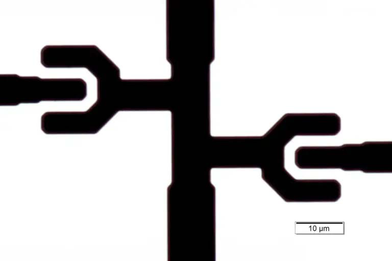
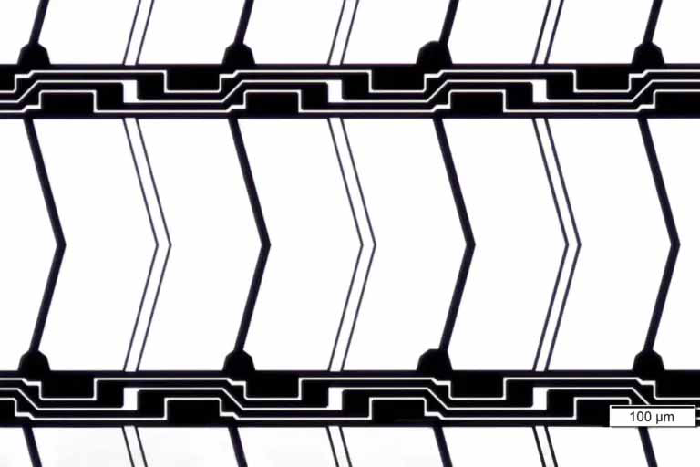
Minimum feature size: Down to 0.75 μm
Address grid: Down to 12.5 nm
Maximum write speed (at structure size 4 um): 13500 mm²/min
Exchangeable write modes
Real-time autofocus system
High power DPSS laser with 355 nm wavelength
Camera system for metrology and alignment
Closed-loop climate chamber
Automatic substrate loading system
Stage map correction
Edge detector system
Multiple data input formats (DXF, CIF, GDSII and Gerber)
Maximum substrate size: 800 x 800 mm² / 1100 x 1100 mm² / 1400 x 1400 mm²
Minimum feature size: Down to 0.75 μm
Maximum write speed (at 4 μm feature size): 16500 mm² / min
Real-time autofocus system
High power DPSS laser with 355 nm
Camera system for metrology and alignment
Closed-loop environmental chamber
Automatic substrate loading system
Stage map correction
Mura correction
Edge detector system
Multiple data input formats (DXF, CIF, GDSII and Gerber files)
曝光速度
100×100 mm²區域寫入僅需9分鐘
曝光品質
邊緣粗糙度<40nm,CD 均勻度<50 nm,解析度< 500 nm
對準精度
第二層正面對準精度達 100 nm,背面 VIS / IR ±1 µm
智慧對準系統
全域/局部自動對準及畸變校正;VIS 背面對準;紅外(IR)對準適用於埋入結構
自動對焦
可選光學/氣動對焦模式,動態補償能力> 160 µm
集成計量功能
即時監測位置、CD及邊緣粗糙度
寫入的穩定性
集成環境計量、流場控制箱和軟體修正功能,以補償環境變化

AVAILABLE MODULES
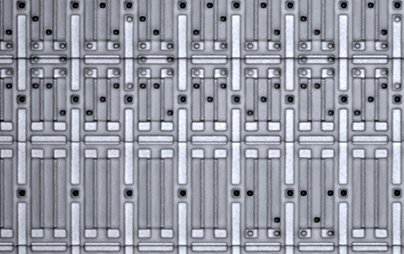
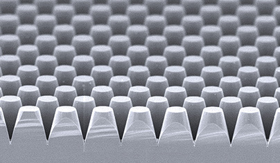
Micro-optics
MEMS
Display
Micro sensor
Micro-optics
MEMS
Display
Micro sensor
Automatic handling options
Open frame handling with SEMI standard carriers and prealigning available for 100 to 200 mm or 200 / 300 mm standard wafers (others on request)
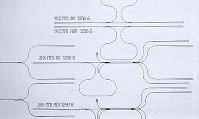
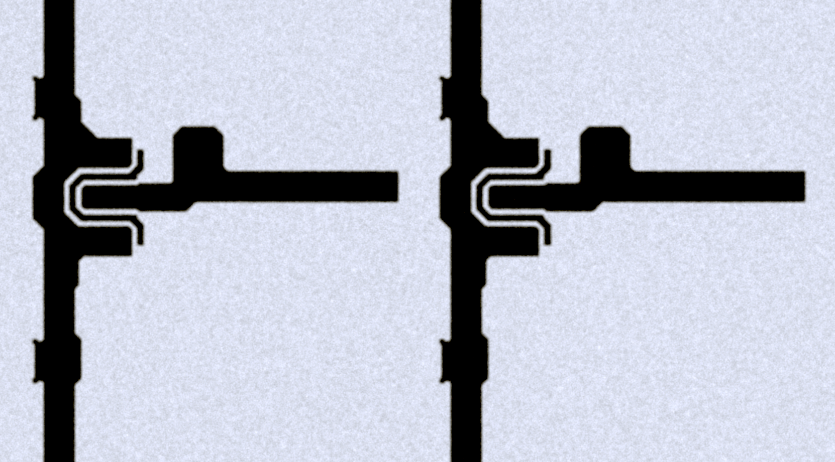
Two write modes to choose from
High NA for highest resolution or lower NA optimized for throughput or DOF critical applications
Alignment options
VIS and IR backside alignment
Service Contracts
Worldwide service level agreements for faster on-site support and access to spare parts