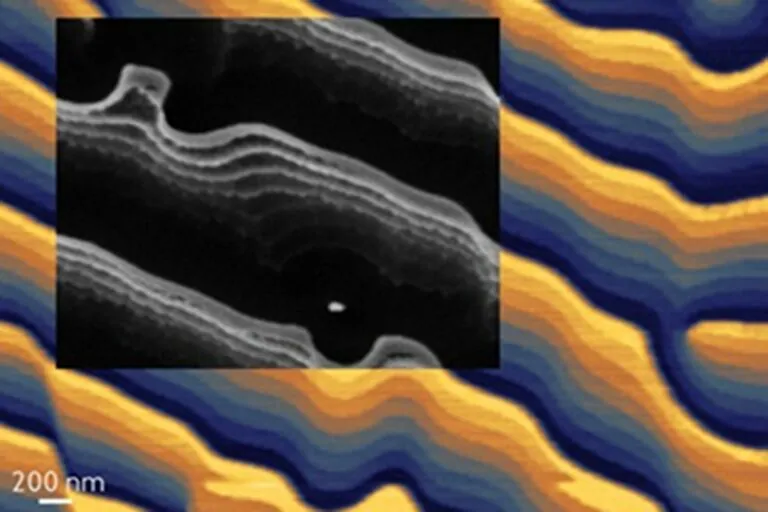
NanoFrazor 是一款突破性的熱探針掃描微影(t-SPL)系統,能夠在多個應用領域進行先進研究,如量子器件、1D/2D材料、量子點、Dolan bridges、Josephson junctions和納米級陣列。它在複雜應用中表現出色,例如灰度光子學、納米流體結構、細胞生長的仿生基質,以及通過加熱進行的任何局部材料改性,包括化學反應和物理相變。
NanoFrazor 的核心特徵是一個超尖銳的可加熱探針尖端,可以同時寫入和檢查複雜的奈米結構;直接雷射昇華(DLS)模組允許在同一光阻中高效地寫入奈米和微結構,並且只需一步製造工藝。
原位成像提供兩個獨特功能:無標記疊加和在寫入過程中比較已寫和目標圖案,這使得參數可以立即調整。這種稱為閉環光刻(CLL)的方法,使任何複雜度的 2.5D(灰階)形狀的垂直精度,達到低於 2 nm;快速且精確的控制加熱的奈米級探針,使得其他技術都難以實現的創新成為可能。
NanoFrazor源自於IBM Research Zürich(蘇黎世研究院)超過20年的研發,現在由 Heidelberg Instruments Nano推進硬體和軟體技術,持續進步。我們的專家不斷優化蝕刻和剝離等圖案轉移過程,針對各種應用建立全面的最佳實踐和資料庫,以支持客戶的需求。
NanoFrazor建立在模組化平台上,可根據特定應用和實驗室環境進行定製。圖案化模式、外殼選項和軟體模組可以結合使用,以實現最佳功能、占地面積和靈活性。隨著研究進展,可以添加升級和附加模式,確保NanoFrazor適應不斷發展的需求。
NanoFrazor革新了奈米製造技術,使複雜的熱探針掃描微影技術(t-SPL) 成為開展突破性研究和技術進步的可行選擇。
為了更詳盡的介紹於 2024 年 5 月首次推出的新世代NanoFrazor模型,我們發布專門的網站,您可以在此了解更多資訊並配置自己的系統:nanofrazor.com。
為什麼客戶選擇我們的系統
「NanoFrazor在奈米微影領域提供獨特的功能組合,集成在一台設備中。我特別強調它在無標記疊加和對二維材料低損傷的拼接方面的優勢,以及在三維灰階奈米微影和材料通過加熱轉換和改性方面的應用。」
— Francesco Buatier de Mongeot
實驗凝聚態物理教授
義大利 熱那亞大學物理系
The NanoFrazor is a groundbreaking commercial system for Thermal Scanning Probe Lithography (t-SPL), enabling advanced research in various application areas such as quantum devices, 1D/2D materials, quantum dots, Dolan bridges, Josephson junctions, and nanoscale arrays. It excels in complex applications such as grayscale photonics, nanofluidic structures, biomimetic substrates for cell growth, and any local material modification through heat, including chemical reactions and physical phase changes.
At its core, the NanoFrazor features an ultra-sharp, heatable probe tip that writes and inspects complex nanostructures simultaneously. The Direct Laser Sublimation (DLS) module allows nano- and micro-structures to be written into the same resist layer efficiently in a single fabrication step.
In-situ imaging enables two unique features: markerless overlay and comparison of the written and target patterns during writing, in such a way that the parameters can be immediately adjusted. This approach, called Closed-Loop Lithography (CLL), results in sub-2 nm vertical precision for 2.5D (grayscale) shapes of any complexity. Fast and precise control of a heated nanoscale tip enables innovation not otherwise feasible with other techniques.
Developed from over 20 years of R&D at IBM Research Zürich and now at Heidelberg Instruments Nano, the NanoFrazor continuously advances in hardware and software. Our experts refine pattern transfer processes like etching and lift-off for various applications, compiling expertise into a comprehensive library of best practices and protocols to support our customers.
Built on a modular platform, the NanoFrazor can be tailored to fit specific applications and laboratory environments. Patterning modes, housing options, and software modules can be combined for optimal capabilities, footprint, and flexibility. Upgrades and additional modules can be added as research evolves, ensuring the NanoFrazor adapts to advancing needs.
The NanoFrazor revolutionizes nanofabrication, making sophisticated t-SPL accessible for groundbreaking research and technological advancements.
To provide a more detailed perspective to the new NanoFrazor model, introduced first in May 2024, we have published a dedicated website, where you can learn more and configure your own system: nanofrazor.com.
WHY CUSTOMERS CHOOSE OUR SYSTEMS
"The Nanofrazor offers a unique combination of features in a single compact instrument for nanolithography. I highlight in particular markerless overlay and stitiching with low damage on 2D materials, 3D grayscale nanolithography, and direct thermal conversion and modification of materials."
Francesco Buatier de Mongeot, Professor of Experimental Condensed Matter Physics
Dipartimento di Fisica, Università di Genova
Genova, Italy