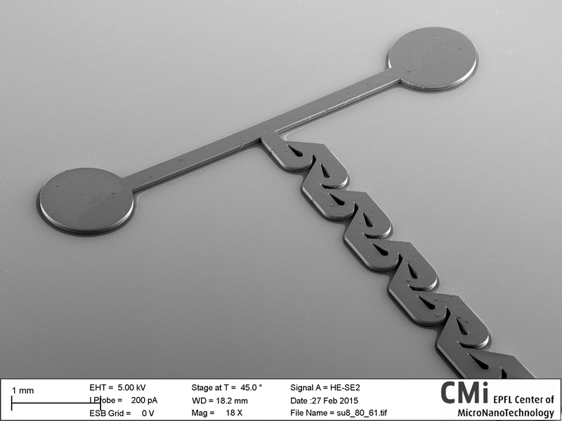
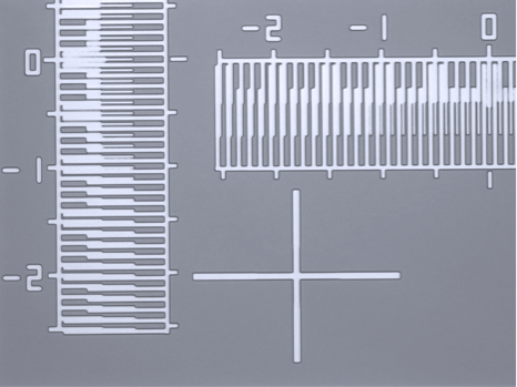
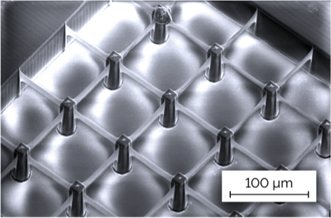
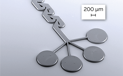
桌上型µMLA系統擁有我們最先進的無光罩雷射直寫技術,是所有需要微結構的研究單位和開發領域的完美入門工具,例如微流體學、微光學、傳感器、微機電系統和材料科學等。µMLA具有前所未有的靈活性和可定制性,並且可支援使用公厘(millimeter)大小範圍樣品。
選擇所需的曝光模式,甚至可以選配兩種模式:光柵掃描光刻模組,快速曝光複雜的圖型;向量光刻模組,創建光波導的平滑輪廓。此外,µMLA提供2種光學設置選擇,具有不同的通量和可變分辨率範圍。在您的光學設置內,軟件可輕鬆切換三種配置,根據您的要求優化分辨率和速度。
NEW: The table-top system µMLA features our state-of-the-art maskless technology and is the perfect entry-level tool for Research & Development, in virtually all areas that require microstructures. Typical examples are Microfluidics, Micro Optics, Sensors, MEMS, and Material Science. The µMLA is flexible and customizable like no other table-top direct writing tool before and supports the use of millimeter-sized samples.
Select the exposure mode you need or even equip your µMLA with both: The Raster Scan Exposure Module provides fast exposure with a speed independent of design complexity. The Vector Module exposes continuous curves, creating smooth contours vital for applications such as waveguides. In addition, the µMLA offers a choice of 2 optical setups with different ranges of throughput and variable resolution. Within your optical setup the software allows easy switching between three configurations, optimizing resolution and speed according to your requirements.
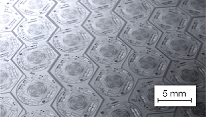
MLA150專為研發及中小批量生產的客戶而設計的雷射直寫系統,滿足實現非接觸曝光、卓越易用性和快速等功能,成為低至中批量生產和研究開發中的理想工具。
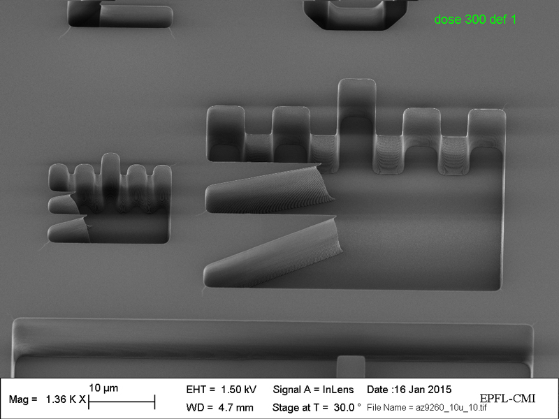
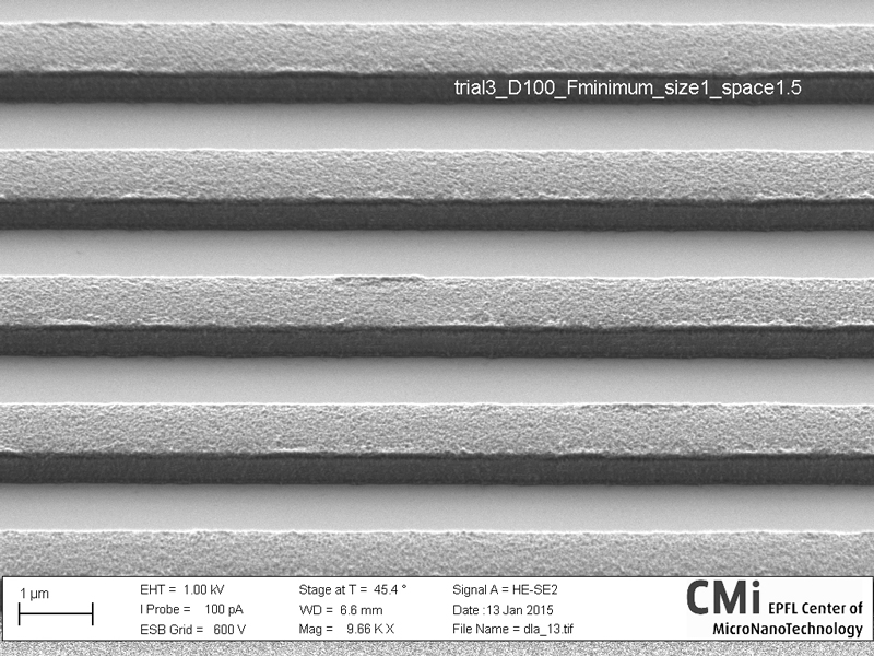
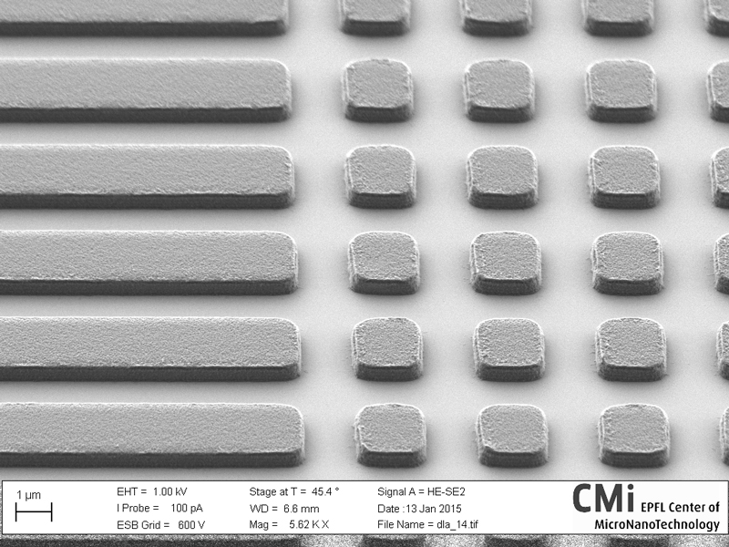
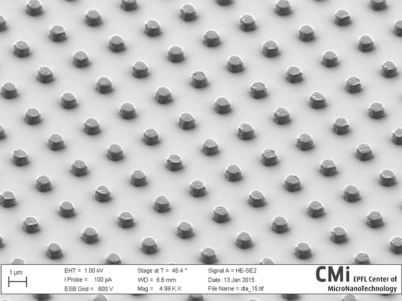
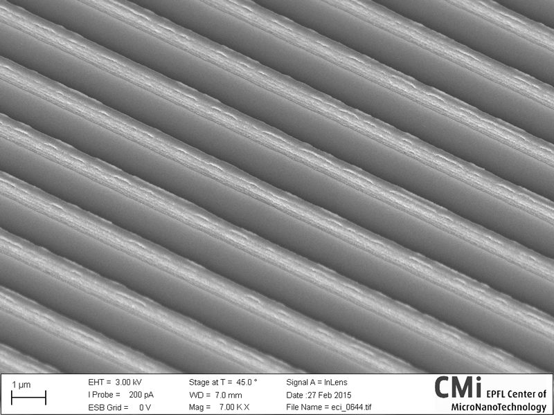
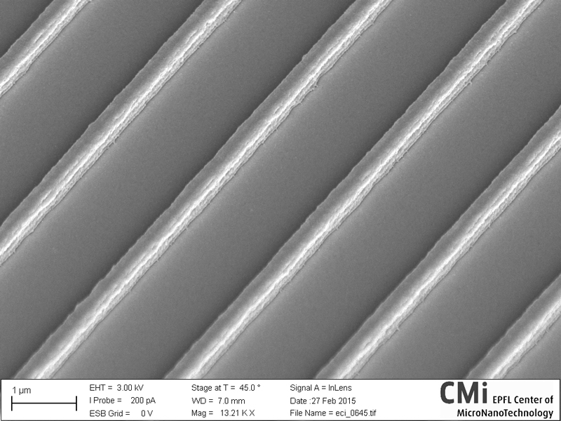
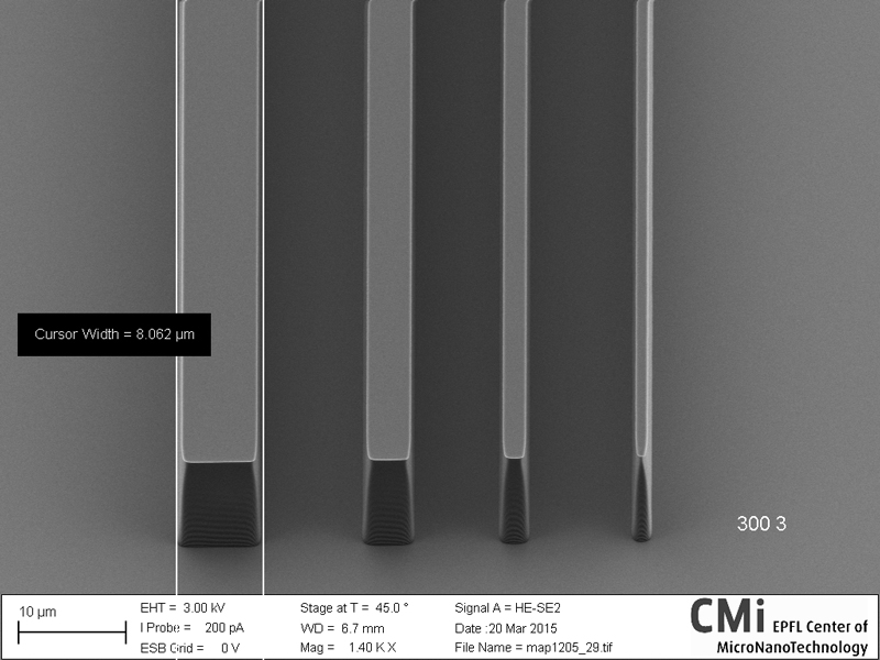
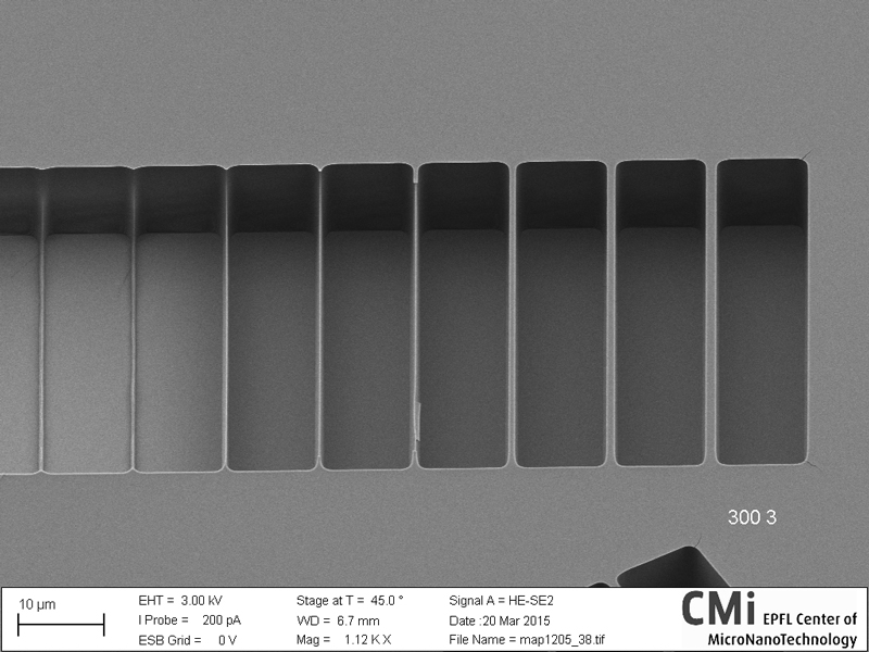
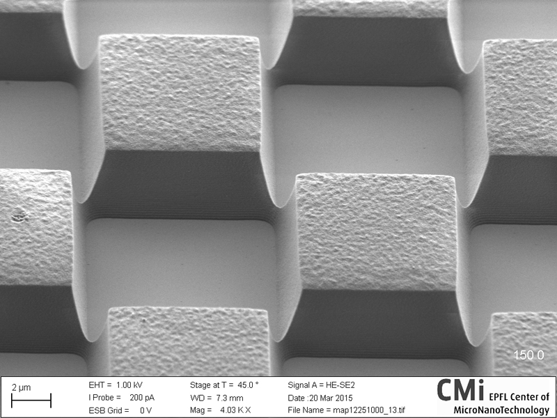
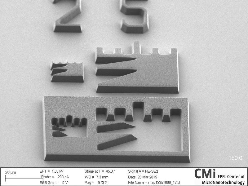
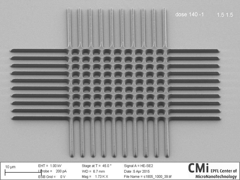
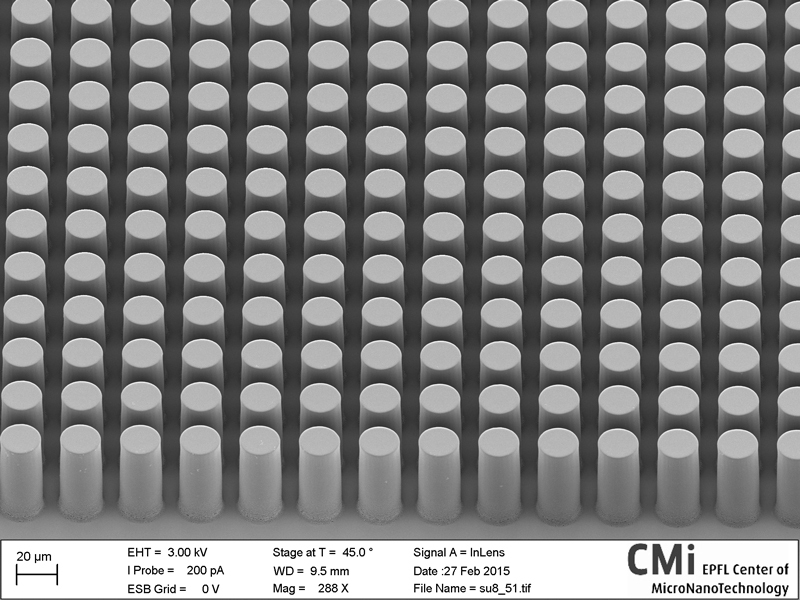
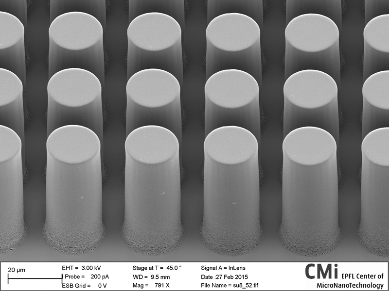
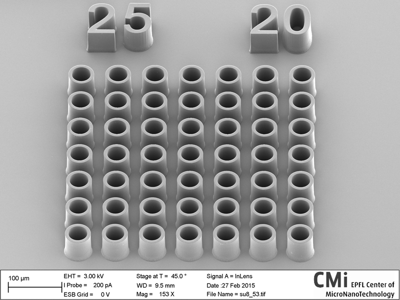
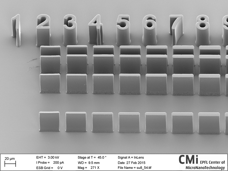
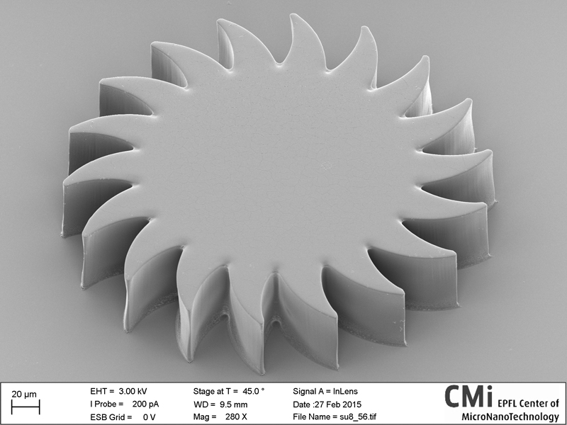
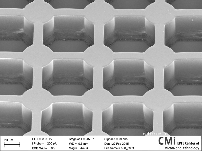
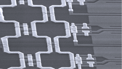
無光罩光刻技術消除了光罩的需求:系統直接將圖案曝光在覆蓋有光刻膠的基材表面上。如果需要進行設計修改,只需要更改CAD佈局即可快速實現,週期時間大大縮短;優點還有快速自動化的正反面對位程序和高效率:曝光100 x 100 mm²的面積,即使是1µm的結構也只需要不到10分鐘。MLA150的應用領域包括生命科學、微機電系統、微光學、半導體、感測器、微光機電系統、材料研究、納米管和石墨烯等科研領域。
Non-contact exposure, outstanding ease of use, and high speed make the Maskless Aligner MLA150 the ideal tool in rapid prototyping environments, for low- to mid-volume production, and in Research & Development. Our once revolutionary, now state-of-the-art maskless technology has become firmly established since our Maskless Aligner series was first introduced in 2015. The MLA150 now presents the modern-day alternative to the traditional Mask Aligner.
Maskless photolithography eliminates the need for a photomask: The system exposes the pattern directly onto the resist-covered surface. Should design modifications be required, these can be quickly implemented by changing the CAD layout, resulting in much-reduced cycle-times. You will also benefit from a fast, automated front- and backside alignment procedure as well as the outstanding speed: Exposing an area of 100 x 100 mm² with structures as small as 1 micron will take less than 10 minutes. The application areas of the MLA150 include life sciences, MEMS, micro-optics, semiconductors, sensors, actuators, MOEMS, material research, nano-tubes, and graphene.
MLA300是Maskless Aligner的工業級別生產系統,已成為研究開發應用、快速原型設計和低至中等產量生產的標準設備。MLA300以高速和高吞吐量實現2µm的最小線寬和間距,並具有全自動化的晶片自動裝取裝置,以及針對生產環境設計的軟件,提供簡單的自動化工作流程;同時,還具備無光罩光刻機的所有優點,省去採購光罩及處理、清潔和存儲所需的費用和開銷。
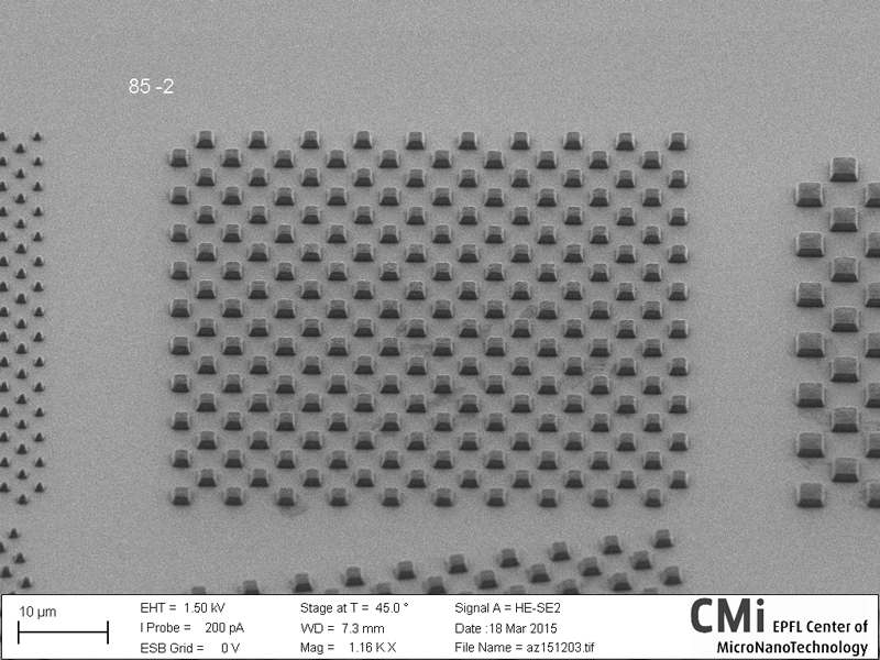
無光罩對位技術使用空間光調制器,如同動態的光罩。它提供具挑戰性的靈活性,允許每個晶片進行圖案校正(例如,對應變形或工藝變化做出反應),並採用實時自動對焦跟踪基板的彎曲或波紋。曝光模式可選擇不同波長(375 nm或405 nm)和分辨率選項,多個曝光模式可以安裝在MLA300中,實現更高的通量產速。
MLA300在生產感測器、微機電裝置、離散電子元件、集成電路、積體電路(ASIC)、功率電子、OLED顯示器以及先進封裝應用等領域表現優異。
The MLA300 is the industrial production version of the Maskless Aligner, which already has become a standard in Research & Development applications, rapid prototyping, and low-to mid-volume production. The MLA300 achieves high resolutions of 2 µm lines and spaces at the high throughput and high availability expected in production. It features full automation with wafer robot and load ports, and software specifically designed for the production environment to offer a simplified automated workflow.
At the same time, it features all the advantages associated with maskless lithography: Overheads and expense associated with the procurement of masks, and their handling, cleaning, and storage are eliminated.
The Maskless Aligner technology uses a Spatial Light Modulator which essentially acts like a dynamic mask. It offers the flexibility to structure the most challenging substrates, allowing per-die pattern corrections (e.g. to react to distortions or process variations), and employs a real-time autofocus to follow substrate warp or corrugations. The fully integrated exposure modules are available for a selection of wavelengths (375 nm or 405 nm) and with different resolution options. Multiple exposure modules can be mounted in the MLA300 for even higher throughput.
The MLA300 excels in application areas such as the production of sensors, sensor ICs, MEMS devices, discrete electronic components, analog and digital ICs, ASICs, Power electronics, OLED displays, as well as for advanced packaging applications.