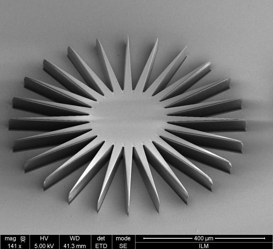
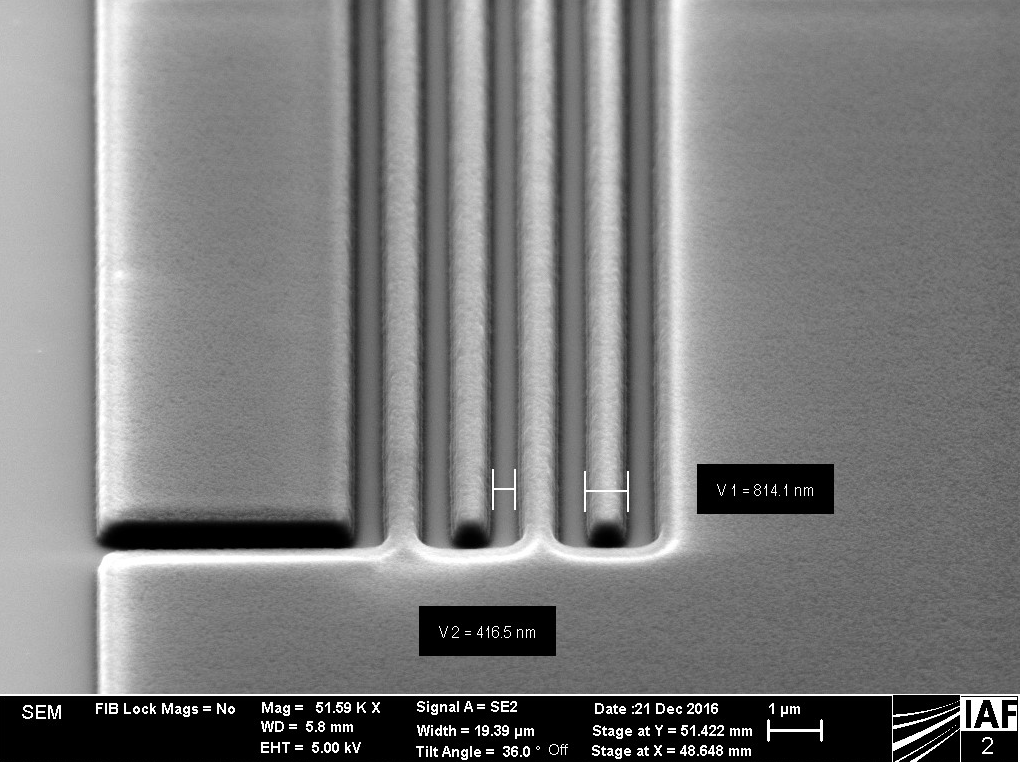
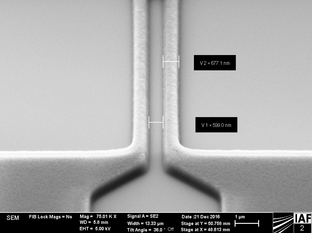
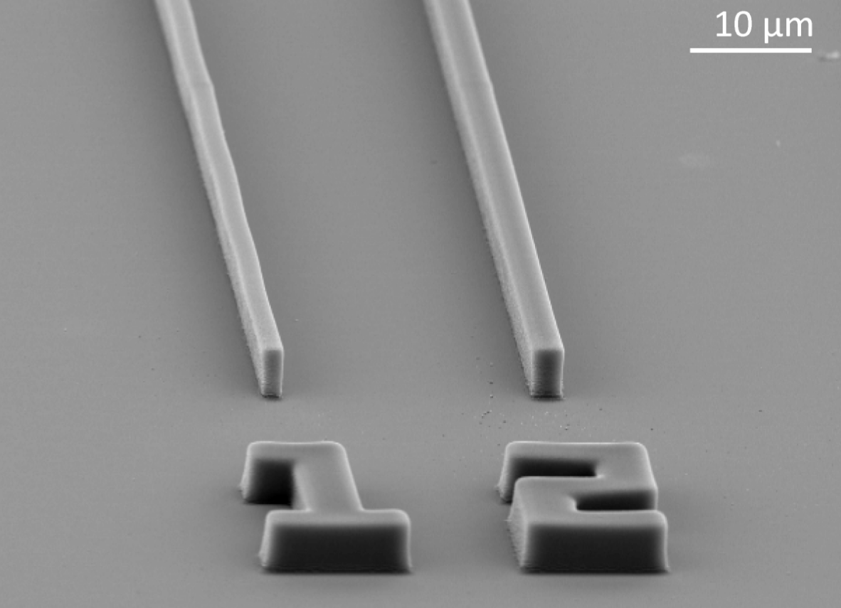
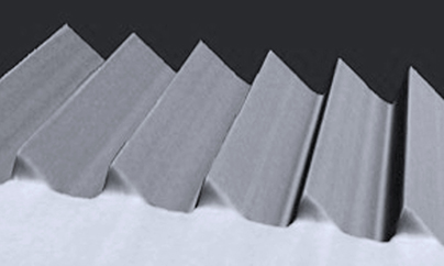
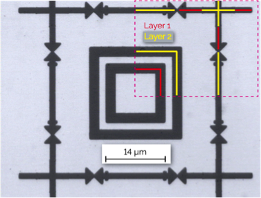
DWL 66+系統是一款經濟實惠、高解析度的雷射直寫光刻機,擁有多種選配功能,例如前後對位和雷射波長可選擇的405 nm或375 nm;進階選配項目有絕對位置校準和自動加載系統。共有六種不同的執行模式可選用,其中包括分辨率為300 nm的高分辨率模式。值得關注的是DWL 66+ 在灰度曝光模式下呈現出卓越的性能,從標準到專業級別:此多功能技術用在低對比度的正型光刻膠厚膜工藝,可以創建複雜的2.5D微結構,例如微透鏡、DOE、全息圖和紋理表面。
DWL66+的高度靈活和可定制的系統,可以根據您的應用特制,運用在生醫工程、先進封裝、微機電(MEMS)、微光學、半導體以及所有需要微結構領域中的必備光刻研究工具。
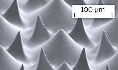
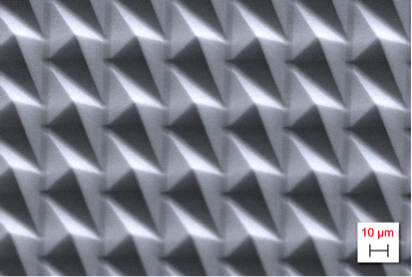
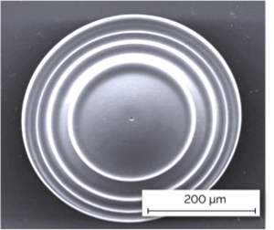
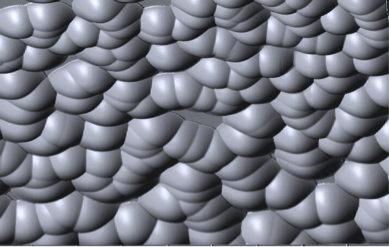
The DWL 66+ laser lithography system is an economical, high-resolution pattern generator for direct writing. The system features powerful options such as front- and backside alignment and a choice of 405 nm or 375 nm laser wavelength. Further advanced options include an absolute position calibration and an automatic loading system. A total of six different Write Modes are available, amongst them the High-Resolution Mode with a resolution of 300 nm. Notably, the DWL 66+ presents the ultimate performance in Grayscale exposure mode, from Standard to Professional levels: This versatile technique for the creation of complex 2.5D microstructures in thick layers of low-contrast positive photoresists is used for applications such as micro-lenses, DOEs, holograms (CGHs), and textured surfaces.
This highly flexible and customizable system can be specifically tailored to your application – the sophisticated capabilities of the DWL 66+ make it the essential lithography research tool in Life Science, Advanced Packaging, MEMS, Micro-Optics, Semiconductor and all other applications that require microstructures.
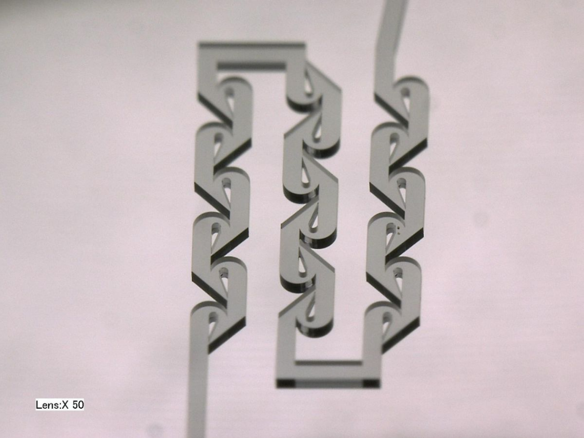
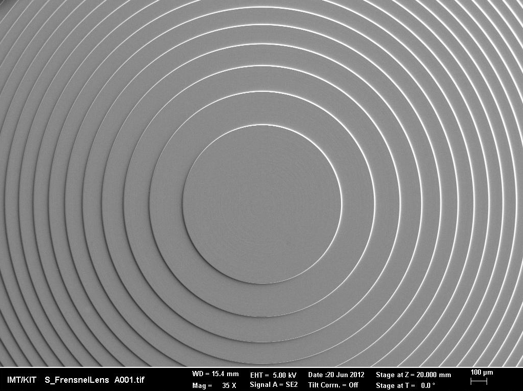
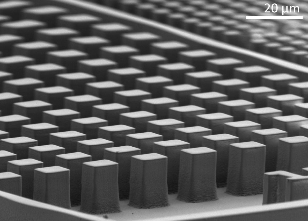
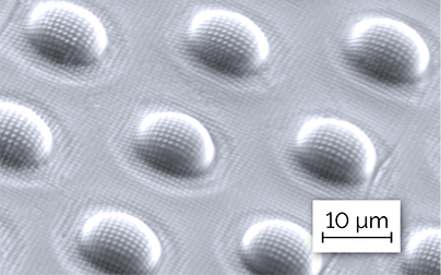
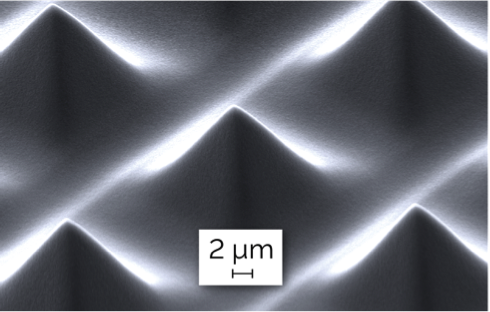
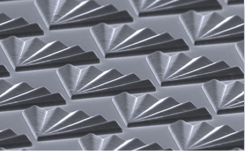
DWL 2000GS和4000 GS 雷射直寫系統具有快速、靈活的高解析度,能夠達到灰階曝光的專業表現。灰階曝光能夠在厚度較大的光刻膠中創建複雜的2.5D微結構。灰階曝光模式的最常見應用包括製造用於通信或微光機電的晶圓光學元件;也被用於顯示器製造和生醫科學設備的製造。
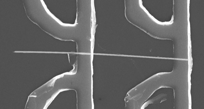
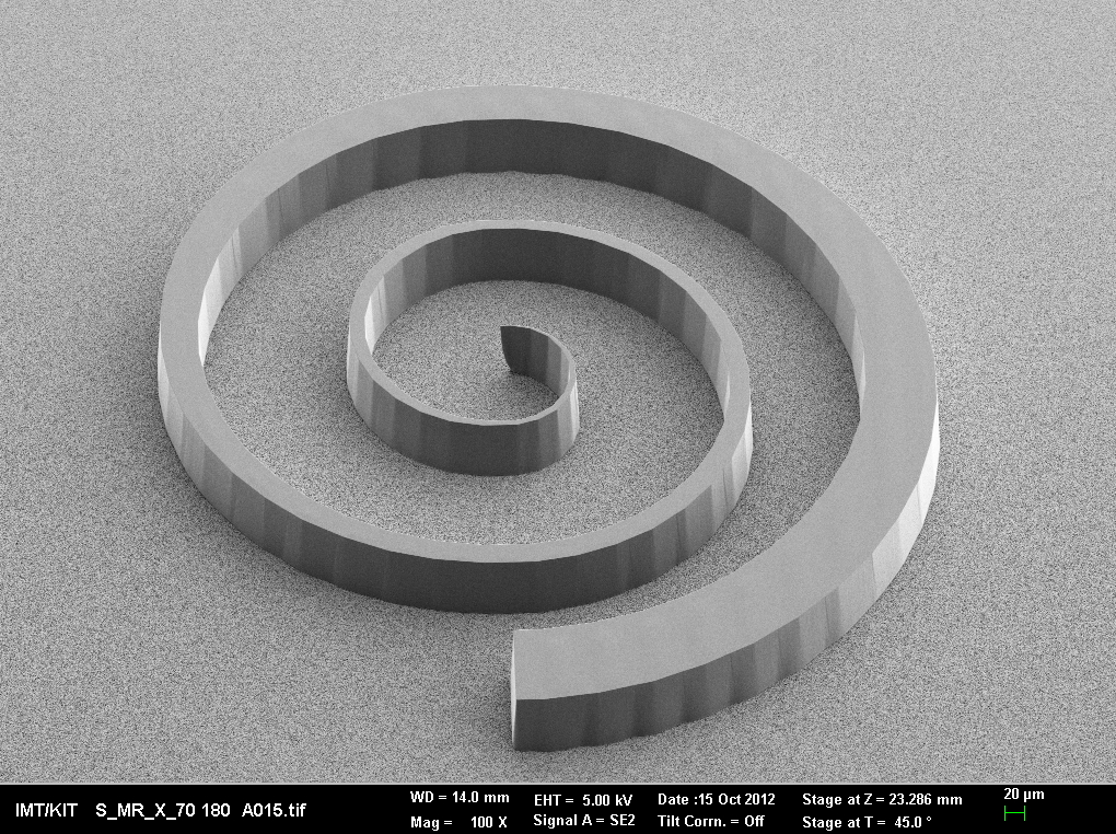
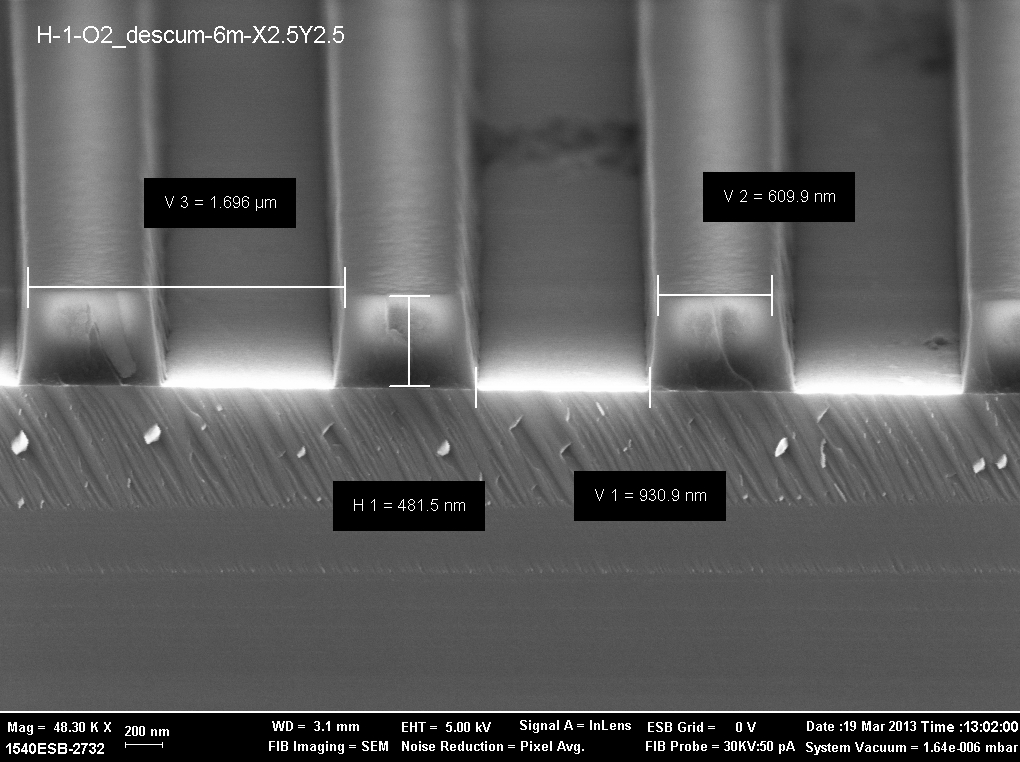
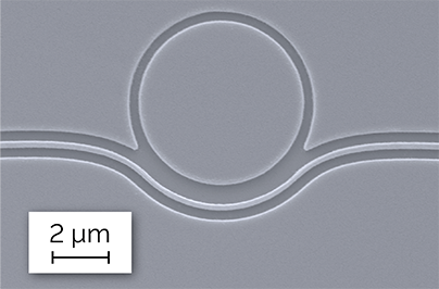
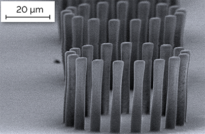
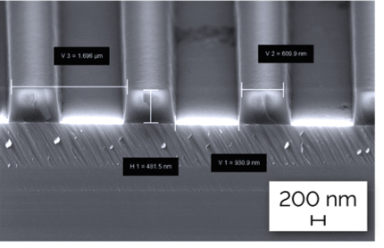
除了灰階曝光外,DWL系列還能以最高分辨率的500 nm最小特徵大小進行二進制2維曝光。這些系統提供了完美的解決方案,如果您需要在微機電(MEMS)、BioMEMS、微光學、積體電路(ASIC)、微流道、感測器和全息圖等領域中,對光罩或晶片進行高通量的圖案,它們的書寫區域可達400 mm x 400 mm,並帶有選配自動載入系統。
The DWL 2000 and 4000 GS laser lithography systems constitute fast, flexible high-resolution pattern generators, capable of the Professional performance level of Grayscale Lithography. The latter allows the creation of complex 2.5D structures in thick photoresist over large areas. Most common applications of the Grayscale exposure mode include the fabrication of wafer level optics used for telecommunication or illumination market segments; it is also used in display manufacturing, and in device fabrication in Biology and the Life Sciences.
In addition to Grayscale, the DWL series tools excel at binary 2D exposures, down to the highest resolution with a minimum feature size of 500 nm. With a write area of up to 400 mm x 400 mm and the optional automatic loading system, these systems provide the perfect solution if you require high-throughput patterning of masks and wafers in MEMS, BioMEMS, Micro Optics, ASICs, Micro Fluidics, Sensors, and CGHs.